Design of RF filter/ RF Combiner
Radio frequency (RF) filter/RF Combiner design continues to face electrical, mechanical and environmental challenges. For example, the system must meet the specified appearance size, the ambient temperature will affect the frequency response drift of the RF filter/RF combiner, and the shell material will also affect the performance of the RF filter/RF combiner. Designers must make trade-offs on the above factors from the beginning in order to design a solution that meets the needs.
There are many existing challenges in designing filters to meet known requirements. These requirements are mainly in electrical, mechanical and environmental aspects. Constraints proposed from system level design, such as mechanical dimensions, are usually of great importance. This paper will discuss the major radio frequency (RF) challenges in RF filter/RF combiner design.
Firstly, an existing product will be used to show the drift of frequency response at different temperatures. This drift of frequency response is very important and should be kept in mind before the beginning of the design process, because the response will change according to the working environment of the RF filter/RF combiner.
Next, the setting of passive intermodulation (PIM) measurement will be introduced. In the process of meeting the requirements of RF filter/RF Combiner products, it may be the most challenging specification. The main reasons include the lack of accurate simulation tools and inaccurate measurement. In order to clearly explain the test process, the block diagram of the test is also provided. The uncertainty in this measurement will also be put forward and some influencing factors will be discussed.
Finally, the trade-off between insertion loss and narrow-band gap suppression is discussed, and some examples of RF filter/ RF Combiner synthesis are also provided to illustrate the trade-off between various requirements. However, under the limitation of considering one and losing the other, it is likely to be unable to meet all the requirements, especially in a limited space. Therefore, the filter designer must ask the customer to clarify the priority between different requirements.
Influence of temperature on filter performance
Here, the effect of temperature on RF filter/RF combiner out of band suppression will be described. Therefore, we take the RF combiner produced by Bri Electronic and Technology Co.,Ltd is a dual band combiner (band 1=698 ∼ 2700mhz band 2=3300 ∼ 3800mhz).
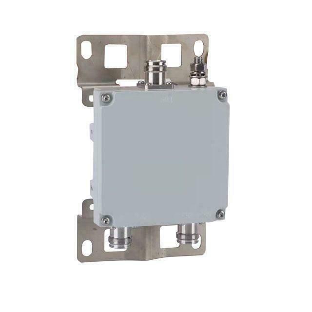
Since the isolation between the frequency bands of this unit is very high (> 50dB), band 1 can be regarded as a dual band filter and band 2 as a simple filter. Since the dual band filter is beyond the scope discussed in this paper, we will focus on Band 2. Incidentally, all resonators in this duplexer are made of aluminum.
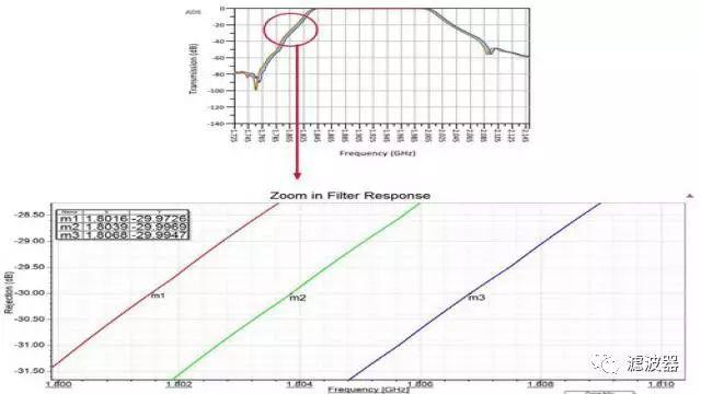
Figure below illustrates the measurement results of this frequency band at three temperatures: – 40 ℃ (low temperature), 25 ℃ (ambient temperature) and + 65 ℃ (high temperature). It can be seen from the figure that the temperature change has a certain influence on the filter. For the known attenuation value (the example in Figure 2 is about – 30dB), it can be seen that the drift from low temperature to ambient temperature is about 2.9mhz, and the drift from ambient temperature to high temperature is about 2.3MHz.
In general, for the center frequency of known materials and combiners, the frequency drift can be predicted by Formula 1:
Δ f= δ Δ T f0 (1)………………………. Formula 1
Among them, δ Is the coefficient of thermal expansion at 10-6 / ℃, Δ T is the temperature change and F0 is the center frequency of the RF combiner.
Apply Formula 1 to some examples, considering δ= 23 10-6 / ℃ (aluminum) and F0 = 1922mhz. At low temperatures, Δ T = 65 ℃, so Δ F ≈ 2.874mhz, while at high temperature, Δ T = 40 ℃, so Δ f≈1.768MHz。
It can be found that the measurement results are consistent with the calculation results of Formula 1. Some errors can be attributed to the shape of the resonator and the interpolation approximation, official account: filter_cn. Therefore, formula 1 can be used to predict the frequency change in the case of temperature drift. CTE δ The value of does not need to be too high to avoid significant changes in attenuation performance, especially for a wide temperature range.
It is important to consider some important factors when selecting resonator materials, mainly including cost, weight, manufacturing method (stamping, die casting, etc.), and silver plating to prevent PIM. Figure below illustrates the tradeoff between the three commonly used materials in the filter.
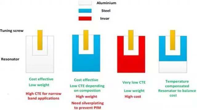
Aluminum is usually low cost and light weight, but the coefficient of thermal expansion (CTE) is relatively high, so it may not be suitable in the case of strict specification requirements. The cost-effectiveness of steel is good, and the CTE is low according to the specific composition, making it a good choice for narrow-band applications. However, steel is a kind of ferromagnetic material and needs silver plating, which will increase the total cost. Invar is basically an alloy of nickel and iron, with high thermal stability, but the cost is also very high.
Temperature compensation for low-cost solutions using resonators of different materials is a common method. This method can find the best balance between the good performance of the final product and the affordable cost.
PIM test for RF combiner and considerations
Here we will introduce the general PIM test setup and outline the various factors that can affect PIM. The block diagram proposed in Figure 4 is a general PIM setting, which can be applied to the device under test (DUT) in this paper. There are two signal generators in the upper left, followed by two identical power amplifiers, which can provide very high gain (usually 50dB). Behind the power amplifier are two isolators, which are basically used to protect the power amplifier from possible high power reflection. Then, the 3dB hybrid Coupler distributes the input signal to two identical paths.
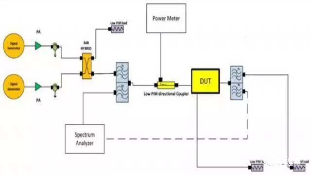
Here, the 50 ohm (Ω) termination of the low PIM is used to terminate one output, and the two frequencies (F1 + F2) sent by the signal generator are mixed at the second output. The directional coupler with low PIM (usually 30dB coupling) is used to measure the power in the input of the device to be tested, and the power meter is calibrated accordingly to read the correct value.
It is generally preferred to use this setting to accurately correct the correct input power, and its error is only equal to the insertion loss of the coupler (about 0.2db). Therefore, two low PIM duplexers are connected in series with the device to be tested. Duplexers also have a high degree of isolation between transmit (TX) and receive (Rx) ports. Any third IMD signal generated will be transferred to RX port and measured by spectrum analyzer.
PIM test can make two kinds of measurements. In reverse PIM, the output port on the filter should be connected to a 50 ohm load with high power and low PIM. On the other hand, as shown in Figure 4, the forward PIM uses a second diplexer, official account: filter_cn, whose TX channel is terminated to a 50 ohm load with high power and low PIM. The third IMD signal will be directly transferred to RX channel, and then measured by spectrum analyzer.
Depending on the stage being processed, there are many factors to consider when operating a low PIM filter. Firstly, in the stage of design and engineering, roughness must be reduced; The contact between metals shall be as smooth as possible to avoid arc discharge. In order to ensure that the latter characteristic can be realized, good silver plating technology is needed to reduce the surface resistance. In addition, it is recommended to adopt sharp edges and avoid sharp spikes on the signal path, such as chamfering technology will help to achieve this purpose. The gap should not be too small, otherwise arc will be generated (generally not less than 1mm). Of course, since ferromagnetic material is an important source of PIM, silver plating is strictly required.
Second, in the assembly stage, any burr shall be removed after the machining of the components to avoid scratching (even partially scratching) the surface of the components. The welding operation shall be as smooth and uniform as possible (e.g. in a homogeneous manner), and the elements shall not be subjected to pressure (bending). The ideal method is to use flange type connectors.
Finally, for the test process, first ensure that the setting itself will not produce PIM, and the input power value should be correct. The connector shall be cleaned and its torque shall be adjusted to about 23 ∼ 24 N.M. The connection position shall be centered. The tuning screw and cover shall be silver plated and tightened with lock nut.
Balance between insertion loss / suppression
For high-power filter modules and wireless site solutions, cavity filter/rf combiner is widely accepted in the industry. For cavity resonators with limited space to design filters, their quality factor is also limited, so it is also a challenge to meet the required insertion loss. Compared with the receiver channel filter, the requirement of insertion loss is more important for the transmitter channel filter, because the higher the insertion loss, the greater the need for larger power amplifier, larger DC power supply and the use of radio radiator.
It is also very common to have high inhibition requirements. In order to suppress the excess out of band power at the power amplifier, this requirement is very important, otherwise the noise level of the receiver channel will be improved. By using cross coupling and increasing the order of filter/combiner and the number of resonators, higher suppression requirements can be met.
It seems simple to solve this problem, but the filter designer must make a choice between meeting various requirements. The requirement to reduce manufacturing costs also brings constraints, such as different mechanical constraints, dimensions, and manufacturing preferences. This will lead to many compromises in the design process, and the choice should be made according to the customer’s priorities.
The example in Fig. 5 is used to illustrate the design of TX filter for duplexer in TX band from 390MHz to 395mhz. Specific requirements include – 85dB suppression in the RX frequency band from 380mhz to 385mhz, and keeping the insertion loss of TX filter below 1.7db. In addition, there are mechanical limitations, such as external dimensions and the location of connectors.
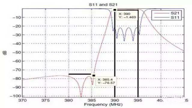
In order to improve the insertion loss, it is not feasible to use the resonator design with a quality factor higher than 2000 because of the limitations of mechanical dimensions, such as the height of the overall structure, manufacturing considerations and tolerances.
Due to the mechanical limitations and the location of the port has been determined in advance, it is difficult to use more cross coupling to achieve more suppression implementation topology. Therefore, more resonators can be used to meet the requirements of suppression and have high insertion loss, or the requirements of insertion loss can be met in Rx frequency band and the suppression can be reduced at the same time.
In these examples, for the design of filter, we should choose between two options, that is, better insertion loss and less suppression, or better suppression and poor insertion loss. This choice can only be made according to the priority of customers. In this regard, we can provide customers with two designs at the same time, explain their advantages and disadvantages, and let them make choices, so that they can meet the more important requirements in case of certain conflicts.
