Basic concepts of RF Power Amplifier
Radio frequency power amplifier (RF PA) is the main part of the transmission system, and its importance is self-evident. In the transmitter’s forward circuit, the RF signal generated by the modulation oscillating circuit is very small. After a series of amplification (buffer stage, intermediate amplification stage, and last stage power amplification stage), enough RF power can be obtained before it can be fed to the antenna to radiate. In order to obtain enough RF output power, RF power amplifier must be used. After the modulator generates the RF signal, the RF modulated signal is amplified to sufficient power by the RF PA, and then transmitted by the antenna through the matching network.
The function of the amplifier is to amplify and output the input content. The contents of input and output, which we call “signal”, are often expressed as voltage or power. For a “system” such as an amplifier, its “contribution” is to raise the “absorbed” things to a certain level and “output” them to the outside world. If the amplifier can have good performance, it can contribute more, which reflects its own “value”. If there are some problems with the amplifier, after starting to work or working for a period of time, not only can it no longer provide any “contribution”, but there may be some unexpected “shock”. This “shock” is disastrous for the outside world or the amplifier itself.
The main technical index of RF power amplifier is output power and efficiency. How to improve the output power and efficiency is the core of the design goal of RF power amplifier. Usually in RF power amplifier, the fundamental frequency or a certain harmonic can be selected by LC resonant circuit to realize undistorted amplification. In addition, the harmonic component in the output should be as small as possible to avoid interference to other channels.
RF Power Amplifier classification
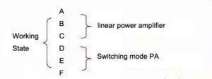
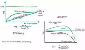
The working frequency of a traditional linear power amplifier is very high, but the relative frequency band is narrow. RF power amplifier generally adopts frequency selection network as load loop. RF power amplifier can be divided into three working states: a (a), B (b) and C (c) according to different current conduction angles. The conduction angle of class amplifier current is 360 °, which is suitable for small signal and low power amplification. The conduction angle of class B amplifier current is equal to 180 °, and the conduction angle of class C amplifier current is less than 180 °. Both class B and class C are suitable for a high-power working state. The output power and efficiency of the class C working state are the highest among the three working states. Most RF power amplifiers work in class C, but the current waveform distortion of class C amplifiers is too large, so it can only be used for load resonant power amplification with tuning loop. Because the tuning loop has filtering ability, the loop current and voltage are still close to sinusoidal waveform, and the distortion is very small.
Switching mode PA (SMPA) enables electronic devices to work in the switching state. The common ones are class D amplifier and class E amplifier. The efficiency of class D amplifier is higher than that of class C amplifier. SMPA drives the active transistor into the switching mode. The working state of the transistor is either on or off. There is no overlap between the time domain waveforms of voltage and current, so the DC power consumption is zero and the ideal efficiency can reach 100%.
The traditional linear power amplifier has high gain and linearity, but low efficiency, while switching power amplifier has high efficiency and high output power, but poor linearity. See the following table for details:

Circuit composition of the amplifier
There are different types of amplifiers. To simplify, the circuit of the amplifier can be composed of the following parts: transistor, bias and stabilization circuit, input and output matching circuit.
1-1. Transistor
There are many kinds of transistors, including the invention of transistors with various structures. In essence, the transistor works as a controlled current source or voltage source. Its working mechanism is to convert the DC energy without content into a “useful” output. DC energy is obtained from the outside, consumed by transistors and converted into useful components. Different transistors have different “capabilities”, such as their ability to withstand power, which is also due to their ability to obtain DC energy; For example, its reaction speed is different, which determines how wide and high the frequency band it can work in; For example, its impedance facing the input and output terminals is different, and its external response ability is different, which determines the difficulty of matching it.
1-2. Bias circuit and stabilization circuit
Bias and stabilization circuits are two different circuits, but they are often difficult to distinguish and the design objectives are similar, so they can be discussed together.
The transistor needs to work under certain bias conditions, which we call the static operating point. This is the foundation of transistor and its own “positioning”. Each transistor has a certain positioning for itself. Its different positioning will determine its own working mode, and there are different performances in different positioning. Some positioning points have small fluctuation and are suitable for small signal operation; Some positioning points fluctuate greatly, which is suitable for high-power output; Some positioning points require less and release pure, which is suitable for low-noise work; At some fixed points, the transistor always hovers between saturation and cut-off and is in the on-off state. An appropriate offset point is the basis of normal operation. When designing a broadband power amplifier, or when the working frequency is high, the bias circuit has a great impact on the circuit performance. At this time, the bias circuit should be considered as a part of the matching circuit.
There are two types of bias networks, passive networks and active networks. Passive networks (i.e. self biased networks) are usually composed of resistance networks to provide appropriate working voltage and current for transistors. Its main defect is that it is very sensitive to the changes of transistor parameters and has poor temperature stability. Active bias network can improve the stability of static working point and good temperature stability, but it also has some problems, such as increasing the circuit size, increasing the difficulty of circuit layout and increasing the power consumption.
The stabilizing circuit must be before the matching circuit because the transistor needs to take the stabilizing circuit as a part of itself and then contact with the outside world. In the view of the outside world, the transistor with a stable circuit is a “brand-new” transistor. It made some “sacrifices” and achieved stability. The mechanism of stabilizing the circuit can ensure the smooth and stable operation of the transistor.
1-3. Input and output matching circuit
The purpose of a matching circuit is to choose an acceptable way. For those transistors that want to provide greater gain, the way is overall acceptance and output. This means that through the interface of the matching circuit, the communication between different transistors is more smooth. For different amplifier types, a matching circuit is not only a design method of “overall acceptance”. Some small tubes with small DC and shallow foundation are more willing to do some blocking when accepting to obtain better noise performance. However, they cannot block too much, otherwise, their contribution will be affected. For some giant power tubes, they need to be cautious in output, because they are more unstable. At the same time, a certain reservation will help them play more “undistorted” energy.
Typical impedance matching networks include l-matching, π – matching and T-Matching. Among them, l matching is characterized by simple structure and only two degrees of freedom L and C. Once the impedance conversion ratio and resonant frequency are determined, the Q value (bandwidth) of the network is also determined. One advantage of π – shaped matching network is that no matter what kind of parasitic capacitance is connected to it, it can be absorbed into the network, which also leads to the universal application of π – shaped matching network, because in many practical situations, the dominant parasitic element is capacitance. T-shape matching: when the parasitic parameters at the power supply end and load end are mainly inductive, T-shape matching can be used to absorb these parasitic parameters into the network.
How to ensure the stability of RF PA
Each transistor is potentially unstable. Good stability circuits can be integrated with transistors to form a “sustainable working” mode. The realization of stable circuit can be divided into two kinds: narrowband and wideband.
A narrowband stabilization circuit is to carry out certain gain consumption. This stabilization circuit is realized by adding a certain consumption circuit and selective circuit. This circuit makes the transistor contribute only in a small frequency range. Another kind of broadband stability is the introduction of negative feedback. This circuit can work in a wide range.
The root of instability is positive feedback. The idea of narrow-band stability is to curb some positive feedback. Of course, this also inhibits the contribution. And if negative feedback is done well, there are many additional gratifying advantages. For example, negative feedback may prevent transistors from matching, and they can communicate well with the outside world without matching. In addition, the introduction of negative feedback will improve the linear performance of the transistor.
Efficiency improvement technology of RF PA
The efficiency of transistors has a theoretical limit. This limit varies with the selection of the offset point (static operating point). In addition, the poor design of peripheral circuits will greatly reduce its efficiency. At present, engineers have few ways to improve efficiency. There are only two kinds: envelope tracking technology and Doherty technology.
The essence of envelope tracking technology is to separate the input into two types: phase and envelope, and then amplify them by different amplification circuits. In this way, the two amplifiers can focus on their respective parts, and their cooperation can achieve the goal of higher efficiency utilization.
The essence of Doherty technology is that it adopts two similar transistors, only one works at a small input, and works in a high-efficiency state. If the input increases, both transistors operate at the same time. This method is based on the tacit understanding between the two transistors. The working state of one transistor will directly determine the working efficiency of the other.
Test challenges faced by RF PA
Power amplifiers are very important components in a wireless communication system, but they are nonlinear, which will lead to spectrum proliferation and interfere with adjacent channels, and may violate the out-of-band radiation standard enforced by laws and regulations. This characteristic will even cause in band distortion, which increases the bit error rate (BER) and reduces the data transmission rate of the communication system.
Under the peak to average power ratio (PAPR), the new OFDM transmission format will have more occasional peak power, which makes the PA difficult to be segment. This will reduce the spectral shielding compliance, expand the EVM of the whole waveform and increase BER. In order to solve this problem, design engineers usually deliberately reduce the operating power of PA. Unfortunately, this is a very inefficient method, because if the PA reduces the operating power by 10%, it will lose 90% of the DC power.
Nowadays, most RF PAS support multiple modes, frequency range and modulation modes, which makes more test items. Thousands of test projects are not uncommon. The application of new technologies such as crest factor reduction (CFR), digital predistortion (DPD) and envelope tracking (ET) helps to optimize PA efficiency and power efficiency, but these technologies will only make the test more complex and greatly prolong the design and test time. Increasing the bandwidth of RF PA will increase the bandwidth required for DPD measurement by 5 times (possibly more than 1 GHz), resulting in further increase of test complexity.
According to the trend, in order to increase efficiency, RF PA components and front-end modules (FEM) will be more closely integrated, while a single FEM will support a wider range of frequency bands and modulation modes. Integrating envelope tracking power supply or modulator into FEM can effectively reduce the overall space demand inside mobile devices. In order to support a larger operating frequency range, a large number of filter / duplexer slots will increase the complexity of mobile devices and the number of test items.