Radio Frequency (RF) probe plays an important role in almost every stage of an RF product life cycle: from technology development, model parameter extraction, design verification, and debugging to small-scale production tests and final production tests. By using RF probes, it is possible to measure the true characteristics of RF components at the chip level. This can shorten the research and development time and greatly reduce the cost of developing new products.
In just three decades, RF probe technology has made amazing progress, from low-frequency measurement to commercial solutions suitable for a variety of applications: impedance matching in 110ghz high-frequency and high-temperature environment, multi-port, differential, and mixed signal measurement devices, high-power measurement up to 60W in continuous wave mode, and terahertz applications up to 750ghz.
The earliest RF probe technology used by people is very different from today’s tools. The early probe used a 50 Ω microstrip line gradually converging from a very short wire tip, which contacts the pressure point (PAD) of the device under test (DUT) through a small hole on the probe substrate. At this time, the technical difficulty lies in how to achieve repeatable measurement when breaking through 4GHz. Although it is possible to eliminate the influence of a relatively large series inductance at the pole tip of a contact line through the calibration process, the radiation impedance of the pole tip will change greatly when the fixture of the circular wafer is moved. The pole tip design used for high-frequency measurement is different from that used for DC and low-frequency measurement, and the 50 Ω environment must be as close to the DUT voltage point as possible.
After that, engineers made a breakthrough in probe technology. The basic requirements and working principle of RF probe are determined:
1) The 50 Ω planar transmission line of the probe shall be in direct contact with the DUT pressure point without contacting the conductor. For the microstrip line and subsequent coplanar probe design, the contact of the probe is realized by a small metal ball, which should be large enough to ensure reliable and repeatable contact.
2) In order to contact the signal voltage point and grounding voltage point of the DUT at the same time, the probe needs to be tilted. This process is called “planarization of the probe”.
3) The contact repeatability of the probe is much better than that of the coaxial connector. It is convenient for the development of probe tip, on-chip standard and special calibration methods.
4) The contact with high repeatability can accurately calibrate the probe and move the measurement reference plane to its extreme tip. The loss and reflection of the probe from the probe line and the transition to the coaxial connector are offset in a similar way by the errors of the RF cable and connector.
5) Because of its small geometric size, people can assume that the equivalent model of plane standard parts is purely lumped. In addition, people can easily predict the model parameters from the geometric dimensions of standard parts.
As the design of the probe changes from microstrip line to coplanar waveguide (CPW), the manufacture of the probe becomes easy (Fig. 1). Tektronix eventually transformed the probe from a “do it yourself” tool into a real product of the emerging RF semiconductor industry (Figure 2). This indicates the beginning of the era of RF measurement at the wafer level.
In the early 1980s, Tektronix launched the earliest RF wafer probe model tmp9600 and sapphire calibration substrate cal96 (Fig. 3). Eric strid and reed Gleason, the main developers of the probe, founded cascade Microtech in 1983 and launched WPH probe. The two companies provided very similar RF probes for several years until Tektronix finally withdrew from the round chip probe business in the early 1990s. Under such an opportunity, with its good relationship with Hewlett Packard, cascade Microtech has become the most important supplier of RF probes in the industry.
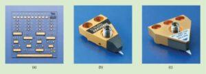
(a) The first commercial sapphire calibration substrate cal96; (b) RF round crystal probe tmp9600 from Tektronix; (c) WPH probe from cascade Microtech.
The frequency of the WPH probe expanded to 26ghz in a short time and reached 50GHz in 1987 to meet the needs of the rapidly developed monolithic microwave integrated circuit (MMIC). The V-band and W-band probes appeared in 1991 and 1993, respectively. In 1988, cascade launched the 26.5ghz series of extremely sharp replaceable probes (RTP) for large-scale production applications. Now, people can quickly replace the ceramic tip without moving the probe body from the test bench. WPH probe has contributed to the development of microwave technology in the 1980s and 1990s, but there are several technical limitations. The most critical limitation is the fragile ceramic CPW line. Even a minimum force above the recommended value (for example, to achieve better contact) can damage the probe. Many engineers call this moment the “voice of death”. The sound of a broken ceramic probe will often push the whole project to a dead end because probes are very expensive for universities and small laboratories. Although RTP series was introduced, ceramic probes were squeezed out of the market by other technologies.
When GGB industries applied for a patent for an RF probe based on micro coaxial cable, 1988 became another milestone. Using micro coaxial cable as an intermediate transition medium has the following advantages:
1) Significant mechanical improvements extend the life of the probe.
2) The damaged probe can be knocked out again in a relatively easy and inexpensive way.
3) Electrical characteristics have been improved.
4) Simplify the manufacturing process.
5) Reduce costs.
In 1993, GGB introduced the W-band probe at the international microwave Annual Conference (IMS) of the IEEE Institute of theory and technology. Their probes reached 220GHz in 1999, and further expanded to 325ghz in 2006 and 500ghz in 2012. Coupled with close cooperation with suppliers, such as Karl suss (later suss Microtech), GGB industries has become one of the most influential companies in the RF market in the world.
Meanwhile, cascade presented a new 40 GHz air coplanar probe (ACP) at the 43rd spring arftg conference in 1994 (Figure 5). Within a few years, ACP probe quickly reached 110ghz (1-mm connector model) and 140GHz (based on the waveguide model), replacing WPH production line. So far, many engineers like to use ACP to detect gold pressure points due to its soft and lossless contact.
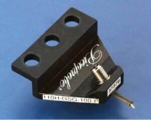 Picoprobe probe from GGB industries
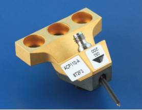 ACP probe from cascade Microtech
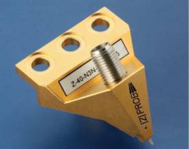 Z ∣ – probe model.
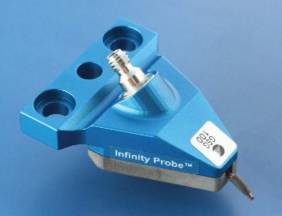 Infinity probe from ascade Microtech
In 2000, the Rosenberger company strongly launched a new concept of RF probe for PCB Applications, which significantly exceeds the traditional technology, reducing the geometric size of the probe to the level required by the round wafer level, and launched a new RF round crystal probe ∣ Z ∣ – probe in 2001. ∣ Z ∣ – the probe can cover the 40GHz range and realize several innovative ideas.
1) This probe does not use micro coaxial cable. The direct transition from coaxial connection to air insulated coplanar contact line is realized.
2) This transition is made in the probe body, which allows an accurate optimization of the transition point to minimize possible discontinuities.
3) This process is similar to the uv-mems process. Its extremely high accuracy and repeatability can form a very accurate shape of CPW line and a constant air gap.
In the mid-1990s, silicon was widely used in the field of RF. This brings some challenges to the fabrication of RF probe. Traditionally, the contact of RF probe is made of beryllium copper (BeCu). This material becomes troublesome when detecting aluminum contact pressure points of silicon devices and circuits. The rapid oxidation of BeCu tip and the accumulation of dirt will greatly reduce the contact repeatability of aluminum contact pressure point. To solve this problem, the supplier provides RF probes with tungsten (W) tips. Test engineers who operate multipurpose measuring devices are forced to replace the probe every time they change the DUT type (silicon or III-V composite semiconductor), even if the frequency range of the test remains unchanged. ∣ Z ∣ – probe is also committed to solving this inconvenience. Coplanar contact is made of nickel (Ni), which shows the best contact performance at the contact pressure point with aluminum and gold. Subsequently, other RF probe suppliers also began to provide multi-purpose probes made of Ni or Ni alloy.
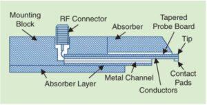
With the increasing demand for RF characteristics of MOS and BiCMOS devices and reducing the size of DUT contact point, cascade Microtech introduced a new round crystal probe based on thin film technology at the 59th spring automatic RF Technologies Group arftg Microwave Measurement Conference in 2002. This method is based on the pyramid probe card technology of cascade company. A microstrip line on a soft polyimide film substrate transmits signals from the coaxial line to the DUT through the tip of a non oxidized rare metal probe. The contact area of the tip of the Ni probe is about 12 μ m x12 μ m. Thus, extremely small contact pressure points can be detected. This new infinity probe demonstrates excellent contact consistency and probe to probe low crosstalk.
Cascade provides infinity probes of different specifications working at 110ghz. Waveguide based probes for 220 and 325 GHz measurements were introduced in 2005 and 2007, respectively. In cascade, infinity probes for the 500 GHz band began to be available in late 2009.
Between 2009 and 2011, two new members entered the mature probe Market: the probe dmpi with micromachining aims at the emerging Asia Pacific Hertz (sub THz) market. Allstron company from Taiwan provides inexpensive probes for applications below 110ghz, among which the reduction of test cost is the most important requirement. The probe from allstron is a traditional design based on micro coaxial cable. The contact structure is air insulated CPW wire. It is similar to ACP, but the pole tip is made into a certain shape to detect the aluminum pressure point with a small passivation window.
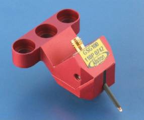 Allstron’s RF prober
The modern design of the RF round crystal probe converts the test signal from a three-dimensional medium (coaxial cable or rectangular waveguide) to the contact of a two-dimensional (coplanar) probe. This operation requires simultaneous interpreting of the characteristic impedance Z0 of the transmission medium and the correct conversion of electromagnetic energy between different propagation modes. Although the input of the wafer probe is a standardized coaxial or waveguide interface, its output (probe tip) can realize different design concepts. These interfaces, especially the tip of the probe, will bring discontinuities into the measurement signal path. This discontinuity itself produces higher-order propagation modes. Therefore, the round crystal probe and DUT excitation must only support a single quasi TEM propagation mode, and exclude high-order modes or show higher impedance to high-order modes.
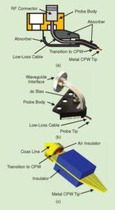
The conversion of the EM field profile is maintained by several RF transition measures in a single probe assembly. A traditional RF probe consists of the following parts:
1) Interface of tester (coaxial or waveguide)
2) Transition from test interface to micro coaxial cable
3) The transition from a micro coaxial cable to a planar waveguide, such as CPW or microstrip line
4) Coplanar interface (or polar tip) facing the DUT on the chip
Several probes either combine 3) and 4) or do not use micro coaxial cable (Fig. 9). A coaxial connector is a common test system interface for RF probes below 65ghz. Both coaxial and waveguide connection schemes are possible interfaces in the frequency range of 50 to 110 GHz. In a single scan, the broadband test system covering DC to 110ghz uses a coaxial connector with a minimum size (1mm). Rectangular waveguides of different sizes are connected with measurement systems above 110ghz.